HR Noise 10: Design Circuit Board
Last Updated on August 2, 2020
First Published on July 15, 2020
So, designing the circuit board of my preamp. I'll use a universal board to make the circuit, and I want to record a placing plot for reproducing.
Here’s how to design placing of electric parts on a universal board using KiCad.
1. Open KiCad (I'm using Ver. 5.1.5 on Windows 10 64-bit), create new project ("File" > "New" > "Project"), then open Schematic Layout Editor ("Tools" > "Edit Schematic").
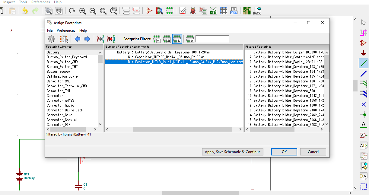
2. Place symbols and wires, annotate schematic symbols (in "Tools" / the left side of the ladybug icon), the ladybug for rules check (or in "Inspect"), then Assign PCB footprints to schematic symbols (in "Tools" / the right side of the ladybug).
3. On the "Assign Footprints" window, select footprints for all symbols. > "File" > "Save Schematic" > "OK" > Close the layout editor, Eeschema.
4. Open PCB Layout Editor ("Tools" > "Edit PCB"). Update PCB from schematic (in "Tools" / the left side of the ladybug icon).
5. On the "Update PCB from Schematic" window, recheck "Re-associate footprints by reference" in "Match Method". > "Update PCB" > Close the window then place emerged footprints in the sheet.
As a 2D CAD, Pcbnew, the PCB layout editor, uses "Grid Origin" in "Place" and selecting the grid pitch for accurate drawing. Circles indicate centers of geometric objects if your cursor in drawing lines, etc. Change the grid pitch to large one if you can't watch centers of any geometry. Note that in "Select Item", the center circles don't emerge. The default grid origin is X 0 and Y 0. "Z" key resets the grid origin. "N" key switches to the next grid pitch, and "N" key holding "SHIFT" key switches to the previous grid pitch (Ctrl+F1 shows Hotkey List). In making PCB, imperial units are dominated because of IC packaging. However in mechanical plots, metric units are dominated. I think Pcbnew accepts both metrics well through this unique method.
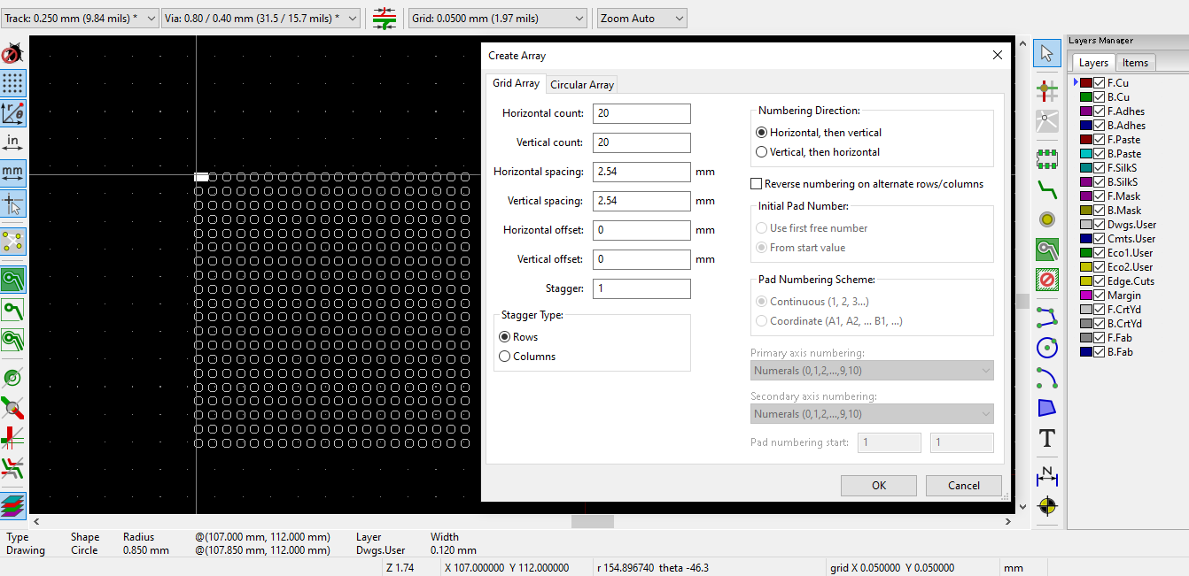
6. "View" > Check "Show Layers Manger". > Select "Dwgs.User" in "Layers". > Select "Grid: 1.0000 mm (39.37 mils)". > "Place" > "Circle" > Click on any coordinate in the sheet. > Select "Grid: 0.0500 mm (1.97 mils)" by "N" key shortcut. > Make a circle with radius 0.85 mm (cursor vertically or horizontally, otherwise the radius is made out of gird pitch). Radius of the circle is shown at the lower left corner of the window of Pcbnew.

7. "Select item" with an arrow icon at the upper right corner. Click the circle you drew. > Right click then "Properties". > Confirm "Radius" and Change "Line thickness" like 0.12 mm. > "OK" > Right click then "Create Array". > In the menu, set counts and spacings of "Horizontal" and "Vertical". Usually, the spacing is 2.54 mm on each dimension. > "OK"
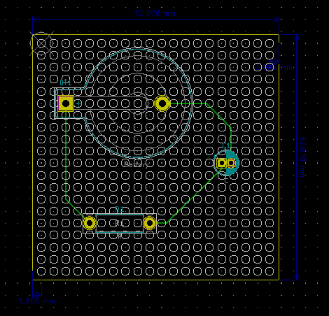
8. Select "Grid: 1.0000 mm (39.37 mils)". > "Place" > "Grid Origin" > Click the center of the first circle. The center is guided by a white circle.
9. Select "Grid: 2.5400 mm (100.00 mils)". > "Select item" with an arrow icon at the upper right corner. Click the footprint you'd like to move. The holes of footprints are guided by circles you drew as long as the first hole of a footprint centers at X 0 and Y 0 coordinates in the footprint editor. > "Route" > "Single Track" > Click any hole of footprints and draw line referencing the guide. Left click to arrange routing in drawing a track.
10. If you want the line edges of the board, select "Edge.Cuts" in "Layers". > "Place" > "Polygon" and draw the geometry. Make sure to set the grid origin to the center of the first circle. By changing the grid pitch, you can draw edges with exact coordinates relative to the center of the first circle. Note that the grid pitch should be any imperial unit (multiples of 0.10 mils) if you set spacing as 2.54 mm. However, dimensions of several universal boards are metric units on these data sheets. I think almost PCB cutters rely on imperial units. So, you can approximate metric units using the minimum grid pitch 0.0025 mm (0.10 mils) in default. However, it costs a lot of time to make the exact approximation of a real board. I recommend that you use 25 mils for the grid pitch to draw edges.
11. If you want descriptions about dimensions, select "Cmts.Users" in "Layers". > "Place" then "Dimension". Left click to point out coordinates according to guiding circles in geometries.
12. Make sure to save your design, "File" then "Save".
-------------------------------------------------------------------
As I described as above, KiCad can change a footprint for a schematic symbol. In my preamp, POTs, etc. are placed on the aluminum box. So, footprints of POTs on the board should be terminal blocks or just holes. I decides to use terminal blocks to wire between actual POTs and the board. However, in an audio circuit, the ground loop on the board should be cut, so parts on the box are grounded directly. That means no need to place holes to GND of POTs, Audio IN/OUT, and DC Power.
I need to make several original footprints to fit with this condition. Footprints of KiCad are licensed under CC BY-SA 4.0. You are free to modify and use existing footprints as long as you don't redistribute these derivatives.
1. Open KiCad. "Tools" > "Edit PCB Footprints"
2. In the "Footprint Editor" window, "File" then "New Library". Make a new library to store original footprints. Ordinary, it's should be created in the project folder, so select "Project" on the pop-up menu.
If you modify an existing footprint;
3. Select any footprints in the "Libraries" menu. > "File" then "Save As". > Rename and select your library you created, "Save".
If you create a new footprint;
3. Select the created library in the "Libraries" menu. "File" then "New Footprint", name something.
4. The drawing method is the same as Pcbnew.
5. Make sure to save your drawing, "File" then "Save".
For example, to match the condition of the circuit board to cut the ground loop, I modified "TerminalBlock_bornier-2_P5.08mm" like this.
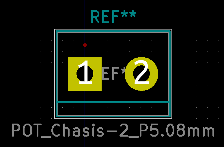
The circle painted by red is actually the No.3 pad. By the way, "Chasis" is French spelling. KiCad is made in French.
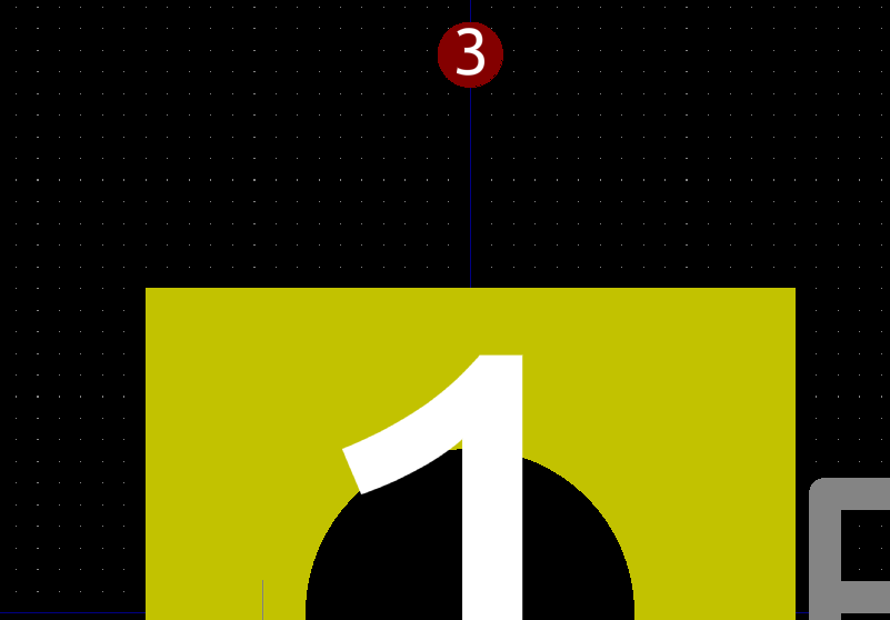
In this photo, the pad is actual copper, but the third pad can be transparent.
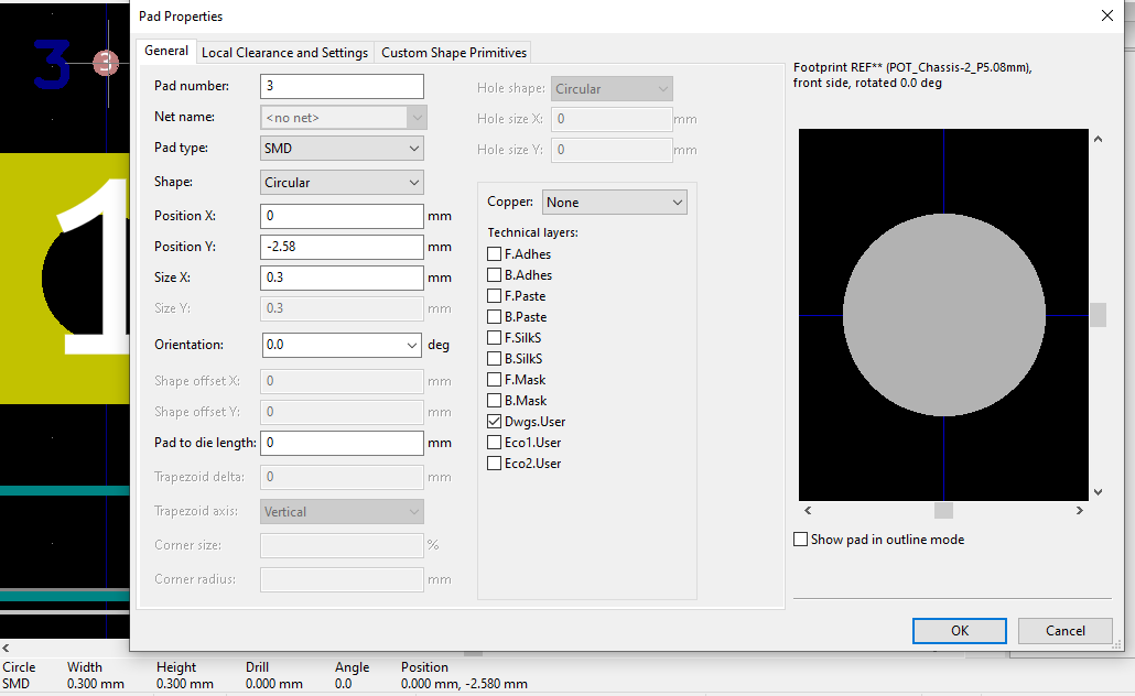
1. Select only the third pad.
2. Right click then "Properties".
3. In the "Pad Properties" window, select "SMD" on the "Pad type" pull-down menu. Select "None" on the "Copper" pull-down menu. Check only "Dwgs.User" in "Technical layers" then "OK". If you select "Through-hole" for the pad type, an error occurs after "OK".
And like this.
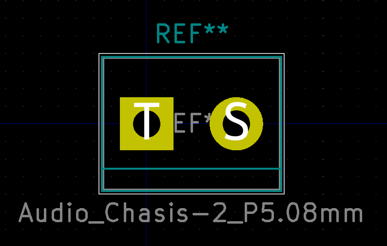
POT's pin names are not numbers. I renamed these to T (Tip) and S (Sleeve).
And like this.
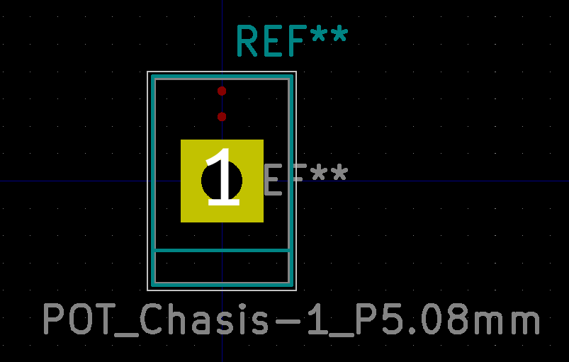
So, I'd like to combine two schematic symbols to a 3-pin terminal block. I modified the footprint to a 1-pin terminal block to connect with 2-pin terminal block. Note that this footprint alarms "Countryyards overlap" in design rules check (the ladybug icon) if you connect this to a 2-pin terminal. However, to be aware of the connection, the alarm can be remained.
-------------------------------------------------------------------
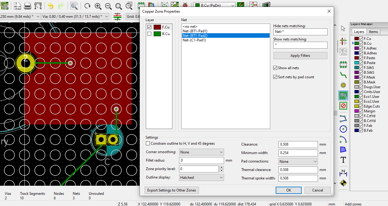
If you plot an audio board in Pcbnew, the GND line should be placed as an actual track with a line because of hiding ground loops. Zone filling with GND is not needed on an audio board. Especially, zone filling with pads directly may not fit with your plot. However, if you want zone filling, placing via holes helps you. Note that this method assumes 2 copper layers. Audio boards should be 1-2 layers. RasPis seem to have 4 layers and more. To change the number of layers, cursor "File" > "Board Setup". In this menu, you can also enable micro via and blind/buried via at "Design Rules". The via type can be changed at "Properties" of each via you placed.
1. "Route" > "Single Track"
2. Left click on a GND track to select. Right click then "Place Through Via" (I assume that GND line is on "B.Cu"). Left click to place the via. Place via holes on tracks connected to GND.
2. Select "F.Cu" in "Layers" of "Layers Manager". Note the track name on the via holes by zooming, e.g., "Net-(BT1-Pad2)".
3. "Place" > "Zone" then left click to point out an edge the zone to draw.
4. In "Copper Zone Properties", confirm that only "F.Cu" is checked in "Layer" and select the name of the track in "Net". In this case, select "Net-(BT1-Pad2)" in "Net", and "None" in "Pad connections". Note that pads with through-holes will be connected with filled zones on all layers if you don't set this setting. > "OK"
5. Draw a polygon for the zone.
6. "Route" > "Single Track" > Delete tracks on the zone. Confirm that the copper zone substitutes tracks.
-------------------------------------------------------------------
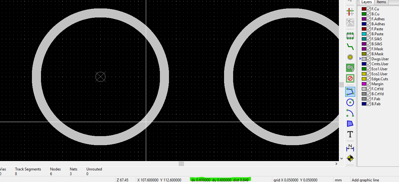
If you'd like to know local references of coordinates in Pcbnew and Footprint editor;
1. "View" > Uncheck "Display Polar Coordinates".
2. Cursor the point you want to be zeros, then press "SPACE" key.
3. The local references are shown up at the bottom of the window. I marked up the references by green in the photo below. I set zeros of X and Y at the grid origin.
-------------------------------------------------------------------
Exporting the PCB design to SVG formatted file saves its actual dimension.
1. Open PCB Layout Editor ("Tools" > "Edit PCB").
2. "File" > "Export" > "SVG". In the "Export SVG File" menu, select "Page with frame and title block" in "SVG Page Size". Select "All layers in a single file" in "Pagination". The blank in "Output Directory" saves the SVG file to its project folder.
3. "Export" then "Close".
SVG files can be opend and printed by LibreOffice.