RasPi 7: Guitar Pedal Effected by Raspberry Pi Pico (Hardware Prototype - Assembly)
Last Updated on January 3, 2021
First Published on September 25, 2021
Previous Posts about This Project, "Guitar Pedal Effected by Raspberry Pi Pico":
RasPi 6: Guitar Pedal Effected by Raspberry Pi Pico (Hardware Prototype - Chassis)
RasPi 5: Guitar Pedal Effected by Raspberry Pi Pico (Hardware Prototype - Initial Report)
RasPi 4: Guitar Pedal Effected by Raspberry Pi Pico (First Half)
RasPi 3: Raspberry Pi Pico Apps
The procedure to mount the board to the chassis is the same as my DIY preamp.
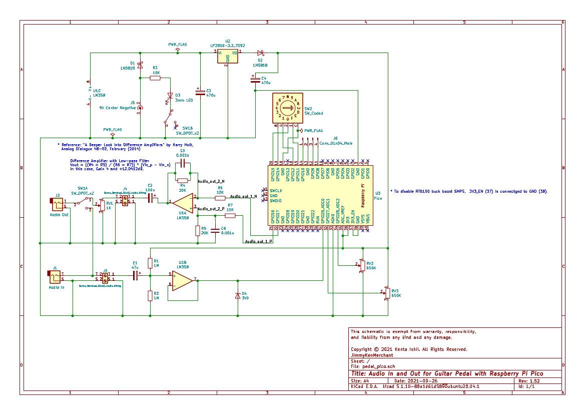
Electrical Schematic
Download PDF File: Schematic of This Project
From my prototype board, I made a layout of an electric circuit board for the guitar pedal project. Changes from the actual prototype board are described as below.
i. Schottky Diode D1: Moved from the back side to the front side. To make a circuit board with etching, all parts are preferred to be placed on a side. Note that I used Schottky diodes with R-1 package, and popular 1N5818 is with DO-41 package which is bigger than R-1 package. I confirmed clearances around these diodes, but I recommend that you actually confirm clearances for big packages. Shottky Diodes which are axial leaded tend to be deprecated or out of manufacture's main line. Diodes with SOD-123FL package seem to be alternative. I assume that 1N5818 drops 0.3V on flowing the current in this circuit, and Pico is driven by 3.0V, but this theory depends on characteristics of a diode. I guess actual voltage to drive Pico becomes in the range between 2.9V to 3.1V. You can change D4 (a Zener diode) to fit with the actual driving voltage you examined. Basically, a Schottky diode withstanding high reverse voltage tends to drop high voltage, and vice versa. However, consuming low current such as 50mA in a circuit seems to flatten the difference of characteristics among individuals and types of Schottky diodes. Note that driving voltage of Pico affects the ADC voltage resolution, and driving with 3.0V is expected to be better resolution than driving with 3.3V (in addition, consuming current in a circuit would be reduced with 3.0V).
ii. Wiring U1 to C2 and RV2 and U3 (Wires Between U1 and U2): Reduced a wire on the front side.
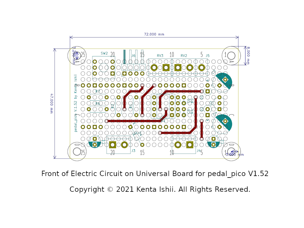
Modified Layout from Prototype
Actual Prototype
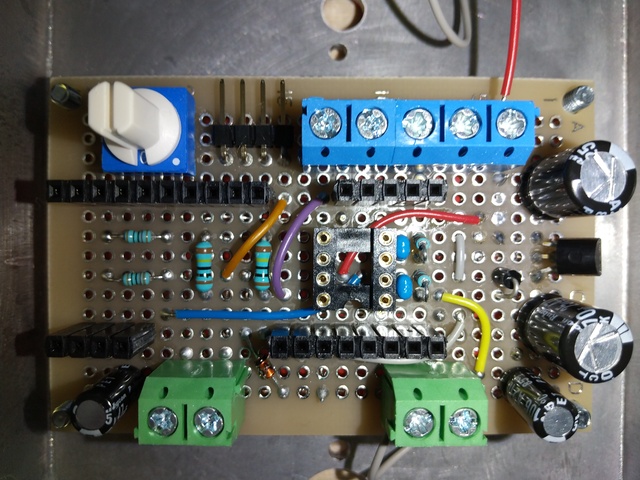
Wires on the front side can be made like "L" curves, but "S" curve is difficult to be made. If you want wires which are thicker than 1.0mm outside diameter (I applied wires with 1.04mm outside diameter though), the IC socket under an Op Amp (U1) would be replaced with a pair of rounded (machine) single row sockets. The photo above shows red and blue wires are close, and the blue vinyl insulates the inner stranded wire against the solder pad for the red wire.
Download SVG File: Universal Board Layout (Front Side)
About lengths of wires on the front side, you can calculate using circles with 2.54mm pitch and Pythagorean theorem. In this case, I placed circles, numbers, and alphabets to indicate a "C" universal board is drawn in the "Eco1.User (Engineering Change Order)" layer on Pcbnew of KiCad because the "Dwgs.User" layer is complementary design in footprints.
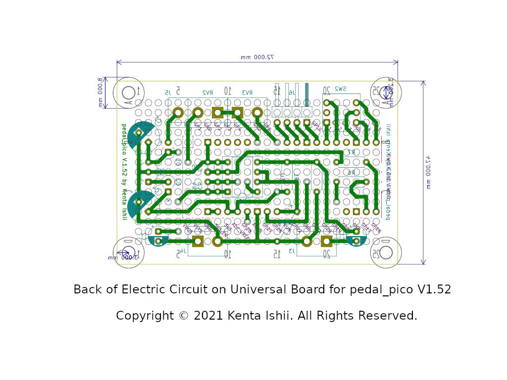
Modified Layout from Prototype

Actual Prototype
Download SVG File: Universal Board Layout (Back Side)
I exported SVG files in Pcbnew (File > Export > SVG). In the "Export SVG File" menu, I selected "Print board edges" and "All layers in a single files". I also selected "Print mirrored" for the back side.
-------------------------------------------------------------------
* (Updated on 1/3/2022) I uploaded another file for a copper clad board. The view is mirrored to transfer ink from a paper to a copper clad board. Small drill marks are useful to know centers of holes to guide drilling.
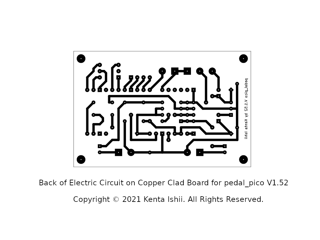
Download SVG File: Circuit for Copper Clad Board (Back Side with Small Drill Marks)
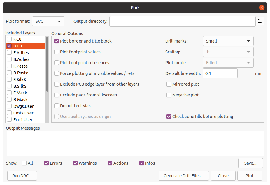
Unlike other files, I exported the SVG file via plotting (File > Plot) of Pcbnew. Settings on the "Plot" menu are applied as shown below.
Caution that I haven't tested making a board by etching. This circuit is just for your reference and my future DIY. In Pcbnew of KiCad, I arranged sizes of pads to [⌀0.9mm or ⌀1.02mm hole / ⌀1.80mm pad] or [⌀0.8mm hole / ⌀1.60mm pad] and vias to 0.8mm / 1.60mm. In datasheet, you can find out how wide the suitable hole is (I widen holes for SW2 rather than instructions in a datasheet to get compatibility). Probably 0.74mm is the minimum pad clearance ("File" > "Board Setup" > "Net Classes" then Design Rules Check). I also changed coordinates ("Position X:" and "Position Y:") of pads. Both can be changed in "Properties (in the menu of a right click)" of a selected pad. "Edit" > "Cleanup Tracks and Vias" is useful to cleanup. Holes on corners are placed using vias with ⌀3.20mm hole / ⌀3.60mm pad, but it's just a guide. To drill holes on corners to fit with a chassis by screws, use the drilling plot.
-------------------------------------------------------------------

List of Parts
I used resistors by Takman which is equivalent from ones by KOA. I used a lead solder, and this can be drained from holes by a desoldering wick. Whereas, a lead free solder can't be drained in my experience. In view of possible breaking parts by your heat iron, I recommend to use a lead solder although lead is hazardous material to harm human body and the environment. Your electric parts are made with emitting CO2 and consuming several materials which may affect the environment.
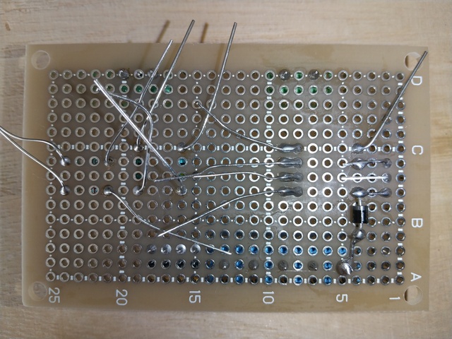
First steps on making prototype.
Started soldering from low parts. As I told you, I spend 4 days to make this prototype board because of keeping my concentration with the draft plot which hadn't achieved. I also used a flux cleaner to keep the fresh looking of the board and my mind. For proper soldering of sockets for a Pico on the board, I used another Pico (see also the initial report including the idea about soldering).
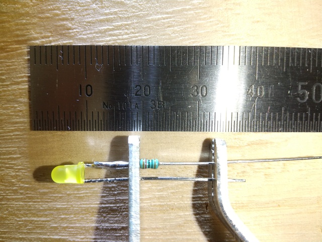
Making a LED unit. A yellow LED and a 10K ohms resistor. Considering the mechanical strength of the LED unit, I soldered the resistor on the anode of the yellow LED, and left the cathode to be wired with SW1. In my DIY preamp, I soldered a resistor on the cathode of a green LED.
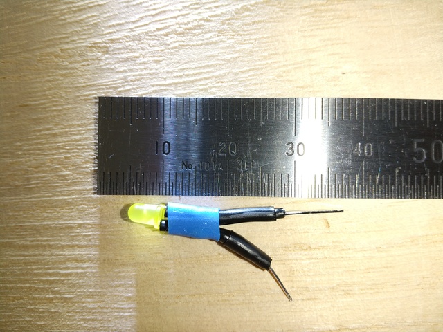
To get the mechanical strength of the LED unit, I used shrinking tubes 1.5mm diameter black and 3.0mm diameter blue. The yellow LED seems to be darker than the green LED I applied in my DIY preamp. The difference could be explained by a luminous efficiency function.
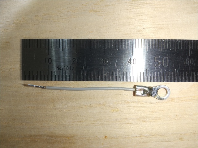
Caution that this is the wrong crimping according to the manufacture's recommendation. No solder, show stripped wire through a crimping hole, and stay stripped wire before a crimping hole especially for automotive which need mechanical strength against vibration.
Wiring the ground of the power jack with a ring terminal, and the 9V with the LED unit. Note that I also applied the same ring terminal to ground the prototype board to the chassis (from J4 to the bottom of the lower right screw as a washer).
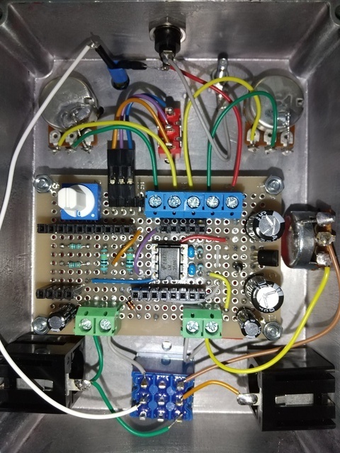
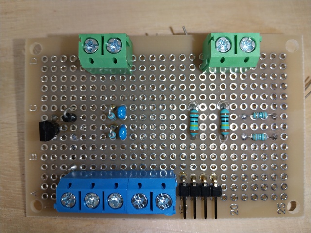
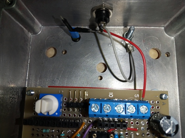
Please refer the image of the actual prototype for wiring board with jacks, potentiometers (POTs) and switches. Basically, I soldered wires with mounted parts on the chassis, but RV2 and RV3 were wired before mounting. On this image, 3 trios of on-off-on pins on 8Y3011-Z (SW1) are vertically lined up. Also refer my rule for numbering lugs of POTs in my schematics. Coating on a metal back of a POT causes wrong soldering for grounding, e.g., floated solder. RV1 at 1K ohms is a new design, having a thickly coated back. To hide wrong soldering, sand the surface of the back to peel off coating, and presolder both a back of a POT and a wire.
* (Updated on 11/28/2021) There are discussions on assembling this pedals on Q1-5: There is no 16mm 1K ohms B curve 1/8 watt POT with a knurled a shaft and solder lugs in any store. What about an alternative of this? and Q1-6: Can I connect headphones to the output jack? in the next post, RasPi 8. Refer to discussions before actual assembling.